Radio receivers based on field-effect transistors. Power amplifier on IRF630 for HF radio station Powerful transistor HF power amplifier
Transistor - 600 W - PA on HF
Introduction.
The article was written during the day, I must honestly admit, in contrast to Sergei’s article - EX8A. Which directly calls everyone to go back (“back” is the direction of movement, and “to the back” is the place of arrival).
However, in addition to my own desire, there were also calls from the reading public: it’s weak to post something specific myself... I answer - not weak. Read. But I warn you that I’m not going to get lost in thought, I won’t teach truisms - everything is in textbooks and reference books, there will be a minimum of lyrical digressions.
1. Review of the situation.
I am sure that the idea of the impossibility of creating a HF PA with a power of more than 1000 W using transistors was invented by supporters of tubes. Probably because it is difficult for them to race against time and change their own thinking patterns. And when they are told that industrial PAs with a HF of 1 kW exist, they answer: they are industrial.
As for the PA on modern lamps, the arguments against it are the fragility and fan noise in the first place. And instead of the modern ones, the GU-81 is offered (this is “backwards”).
2. Durability.
I don't understand why it is claimed that the longevity of modern lamps is worse. The reference books indicate exactly the opposite. Does anyone deliberately put “false” information in reference books? Or do the authors of this “idea” simply have no other way but to turn everything upside down, calling into question the data of the reference books? And the answer is simple - there is no other way to justify the need to create a design based on OLD lamps, which not only have been discontinued for a long time due to “unsuitability”, but which have long since expired all conceivable shelf life.
Modern ones, you see, we need to train, but what about these shaggy GU-81s? Well, of course, it’s impossible to say that they don’t need to be trained, which is why they bashfully say that it won’t be any worse if they are also trained, and then they describe in detail the technology of the entire procedure.
3. Fans.
Everything is quite simple here: GU-81 fans are not even interested in knowing what modern fans exist there. But if you think about it, there are 1-2 fans in the transceiver power supply (in my GSV-4000 there are two fans), in the transceiver itself there are 1-2 fans (in my IC-781 there are 4 of them), in the computer there are 1-2 fans. A total of 3-6 fans operate continuously. And - nothing, they don’t interfere, no one remembers about them. Why? Because there are fans that have a noise level of 22-26 db. It's at 10!!! times quieter than a quiet conversation. Feel the difference! And they already “know how” to pump decent volumes of air. And what cool “snails” we have now! And they can also be paralleled (according to the air flow)... But if you don’t know about this, then you can, of course, criticize the VN-2 and the like. I listened to the noise of the ACOM-2000A fans, I’ll tell you: nothing buzzes, nothing interferes, nothing distracts, and it delivers 2 kW, and there is an automatic tuner, and eight microprocessors service the entire monitoring and control process. And the sizes...! And only 2 pieces of GU-74B. Will we compare further with the GU-81?
4. Power supplies.
What happens if you “short” the plus of the power supply with the minus? That's right - there will be a spark. The greater the power of the power source, the larger the spark. The spark parameter is its energy (roughly, this is the instantaneous power that the power source can produce). Now let's look at the power supply for the PA anodes on two GU-81s. This is a voltage source of 3000 volts and a current of 1-1.5 amperes. Now look at the power supply of a 1000 watt transistor amplifier. This is a voltage source of 48 volts with a current of about 50 amperes. Whatever they say, the spark energy from these sources will be approximately the same. True, there is a difference - try to touch (by accident, of course) the plus of the transistor PA source - but nothing will happen to you, and try, also accidentally put your finger on the anode. In the second case, have a will written in advance.
The weight of the power supply for 2 GU-81s is scary to think about, probably 30-40 kilograms. What about the dimensions? It would be interesting to see the photo.
The power supply for a transistor amplifier has such a characteristic as specific volume. This is 2 liters of space volume per 1 kW, and the weight is only 600-700 grams per 1 kW.
5. Cost.
A pertinent question. Ask on the Internet how much a GU-84 amplifier costs from well-known home-made “manufacturers” - the answer is simple - at least 2000 USD, and for a GU-78B it’s just 100,000 rubles. And then – no earlier than in 2-3 months you will be able to receive it. True, we must honestly say that everything was done well, soundly, and for a long time. There is already experience in long-term operation of such amplifiers - 5-7 years without breakdowns and replacement of lamps (lamps - to the displeasure of GU-81 fans - metal-ceramic, modern lamps). Who said that an amplifier with transistors of the same power should cost less? And if you make it yourself, it really and truly costs less. A recent example: one radio amateur from St. Petersburg bought a GU-91B with a socket and a fan for 450 USD, for an amplifier that was made in Ukraine for 2000 USD. The price for a used ACOM-2000A starts from 3500 USD. Would you like to ask a GU-81 UM fan how much he would sell it for? At best, he will say that he is not for sale.
The price of a selected pair of transistors for a 600-watt PA is in the range of 250-300 USD. This time. BP – pulsed. I use 2 computer power supplies of 750 watts each. A pair costs 150 USD. That's two.
Of course, there are no 10 pieces of relays P1D or B1B, or even B2B. There is no range switch. There is no stupid P-circuit setting, but this is one or two capacitors and a variometer. And so on, with all the “stops”. That's three.
The rest of the cost of the entire PA increases slightly due to the price of the housing, filter, bypass relay and other small things.
If, using an adder, we add up the powers of two output stages of 600 watts each to get 1200 watts at the output, then, consequently, all costs must be almost doubled. Where can I buy a 1200 W PA for 900-1000 USD? And with such dimensions and such weight? The answer is nowhere.
6. Scheme.
Nothing special, no “tricks” - the most common push-pull circuit.
On one board there is a mind.
Or like this:

Look in more detail:

on the second there is a bypass relay, on the third there are output range filters, on the fourth there is a source of bias for the base circuits. Supply voltage – 48V. The quiescent current of the output stage is 150-250 mA. Transistors TH-430pp. Ferrites – TDK. The windings of the output transformer are stranded silver wire 2.5-4 mm2 (no more than 1 meter).
Adder transformers are a separate topic. Since the diagram can be found in any literature, I do not present it. I show detailed photographs - everything should be clear.
Here everything is assembled on the radiator:


7. Element base.
Again, nothing special - powerful transistors, transformers.

7. Prospects.
With this ONE “handsome” you can get 400-600 watts per HF.

A push-pull circuit will easily deliver more than 1000 watts. Two modules will give more than 2000 watts. The weight of one 600-watt module is 2 kg (with radiator and fans). The weight of one power supply unit is 0.65 kg. Case – weight 1.5 kg. The surface area of the radiator is about 2000 cm2; the side fins are blown through by two computer coolers. In total, everything weighs less than 5 kg.
I would also like to make this automatic and inexpensive 200 W tuner work with a power of about 1000 W, replacing the elements of the matching device with more powerful ones.

Microphone HEIL SOUND HM-10-5 with two “tablets” (different frequency ranges) is here for an understanding of the dimensions.
This is an industrial 500 watt amp on two MRF-150s I took out ;).

And this is its other side.

It was not possible to quickly find a 1 kW industrial amplifier of the same design, only its radiator fins are three times higher, and the board has two parallel amplification channels with an adder between them at the output.
QUESTIONS???
Part 2. Transistor - 600 W - PA on HF
Thanks to everyone who responded to the article. Even to those who thought that I was a rogue, and this article was nothing more than a “scam” and deception.
Fans. Wonderful article by N. Filenko. UA9XBI here on -, I don’t see any point in quoting and repeating. I can only give some figures for orientation: The average hard drive produces noise (average between the standby state and the search state) at a level of 30-35 dB (decibels). For comparison: a whisper - 10-20 dB, a calm human voice - 50-60 dB, a moving train - 90 dB, a plane taking off - 120 dB, pain threshold - more than 130 dB. As for combat use: office noise (printers, faxes, copiers, etc.) - 50 dB, noise in a living room - 30-40 dB, computer fan noise- 20-34 dB. If you want to buy a normal fan, please: http://www.zifrovoi.ru/catalog/coolers/all/
Photos. It seems that this is precisely where some are trying to find the catch. I ordered and bought the first board in Japan, and I posted these same pictures only because they were made more beautiful on a blue background (I think so). There is no secret to this. But if someone thinks that this is not so, please use the same board (again with my microphone).

Power. Now I will film everything on my sofa J). Here's another mind

The output power by range is written on a piece of paper attached to the board with a wire. The resolution of all photographs is sufficient to allow you to examine everything in great detail. What we see there: in the ranges of 7, 10, 14, 18 MHz it produces 500 watts. You see it says there - with a supply voltage of 28 V and an input power of 10 W on all ranges.
At 3.5 and 21 MHz, respectively – 320 W and 400 W. At 1.9 MHz - 200 watts, 24 MHz - 240 watts, and at 28 MHz 160 watts. Thus, at a level of -3dB (which is half the power), the frequency range of the amplifier is 1.9 – 24 MHz. Doubling the power changes the S-meter signal level by only 0.5 points. At a frequency of 28 MHz, the level of the received signal will drop by 0.7 points. By the way, it should be noted that the antenna opening angle is determined in the same way - at half power level, i.e. at a level of -3dB.
In order to increase the output power by 1.9, 24 and 28 MHz, you simply need to increase the input power by 2-3 times (20-30W). Or make an ALC system - automatic power level control. I didn't do this because... I find it easier to turn the RFPWR knob.
This power is provided by the board you see in the photo. I have no doubt that when powered from a 48 V source, and with design optimization of transformers, this board can deliver “a little more” power. And if you add a couple of such modules, you have 1000 watts. Now think about it, is it worth striving for 2000 watts if, in the end, you get an increase in the signal level at the receiving end of only 0.5 points? An example of my neighbor’s work, I won’t give his call sign. On 20, I receive it at 9+50dB (the S-meter is calibrated), and I hear the second harmonic at 28 MHz at 9+5dB. The person has a good antenna (biggun5 el), but the amplifier... is made impeccably, neatly, beautifully, it tells everyone that I have “two hundred kilos” of honest money. And there are two GMI-11 lamps in parallel and an anode voltage of 2500 volts. How is that? Fine? No amount of persuasion helps. And even though a good engineer himself understands that reducing the level by 0.5 points is nonsense, he does NOTHING.
I have a GU-73P amplifier, cooled with some kind of coolant. And the power supply for it, which I was too lazy to photograph. I have never turned it on (it delivers 2500 watts), the power supply weighs about 50 kg. They wanted to somehow steal it because of the aluminum casing, but they couldn’t lift the hi-hi.
Power supplies. First, a photo of a pulse power supply from a well-known American company

This UPS provides 20 volts and 125 amps, for a total of 2500 watts. Weight – approximately 12-15 kg. When examined on the table of the RZ3CC, it turned out that it was absolutely not suitable for our applications. At the moments of switching key transistors, such pulses jump that it becomes even uninteresting to look for options for protecting the receiver from them. True, it must be said that this was a development approximately 15 years ago, and then, of course, they did not yet know about resonant UPSs. The bottom line is that the operating principle of the converters that are used in power supplies for modern transceivers is not suitable for high powers.
Now let's look at the UPSs that I use.
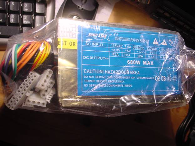
This is understandable - a computer UPS. For those who said something about high currents - enlarge the picture and see the inscription 5v/50a - no bolts and nuts. What I mean is that nothing prevents you from making a connection, for example, even with a ribbon cable.

There are two UPSs here, the top 5V/20A, the bottom 5V/90A. The progress is noticeable - UPSs have become noticeably smaller and lighter. In the IC-781 500W UPS, the power supply has very small dimensions and weighs about 1.5-2 kg, but it is already more than 15 years old. Agree that technology has come a long way.

A 750 W UPS for a computer already has two 12V/22A windings. Take two of these UPSs and get 48V/22A of power input. Just don't forget to decouple the sources with diodes. If you do a little magic with other voltages of these UPSs, you can get an input power of 1600 watts.
My output stage worked with a traditional transformer power supply, in the photo below you see the bus with which the OSM -1 1.0 is wound, by the way, its price on the Internet is 2930 rubles.

Winding with such a bus does not greatly increase enthusiasm, and the weight of the transformer is quite considerable.
I have already said that I have a NORMAL attitude towards lamps; they will be out of competition in the industry for a long time. But I still want something more compact and lightweight. It turned out that they do it, although not for a wide audience. At one research institute I was offered a pulse power supply for a tube PA. They said this: 3000v, 1.5a, in a case, with protection, with the highest class of reliability, in a volume of 3 liters, weighing 2-3 kg, all elements are imported (ferrites only Epcos), for 30,000 rubles, for 1 month. I asked if I could see the diagram, the answer was 15,000 rubles, and the diagram with a detailed description is yours. I didn't buy the circuit. But I realized that there are very interesting options for radio amateurs.


This is a kilowatt module on two GI-46Bs. Fans and heatsinks from the processor. The radiator area of each lamp is 850 cm2, which is almost twice as large as that of the “native” radiator. This idea has been stopped in its implementation for now, due to the emergence of an alternative - on transistors.
Scheme. I will give both diagrams that I received.


As I said - nothing unusual - the most standard schemes. The quiescent current of each transistor is 150-250 mA. As for ferrites, I would strongly advise against using our ferrites at all. There is only one reason - instability of parameters. Red has several options for ferrites - choose any one that suits the power and frequency. Output transformers: I have several options - blue ferrites are AmidonFT-23-43, diameter 23mm, material 43, 6 pieces in each column. 4 turns of wire with a cross section of 1.5 mm square. In the second ring amplifier TDKK6a.77.08 the outer diameter is 28mm, the inner diameter is 16mm, the ring height is 8mm. Two rings in each column. Four turns of stranded silver wire, with a cross section of 2-2.5 mm square. Input transformers – rings internal. Diam. 14-16 mm, internal – 8 mm, column length – 14-18 mm, material M600NN. Four turns of wire with a cross section of 0.35 mm square. The dimensions of ferrite rings in transformers depend solely on the power losses. It is for this reason that, with precise matching, the ring sizes can be very small. As an example, the following photo shows a block of bandpass filters from 500 W, ICOM, which was given to me by RZ3CC (G. Shulgin).

Remember to install high voltage ceramic capacitors where they are indicated on the diagram.


Shown here are measurements of output power versus input power. Not my measurements. The first picture is American, the second is Japanese. But the order of power is absolutely obvious, I would say noticeably better than on the GU-74B, and only two 2SC2879. Well, look at the last sign from the Japanese - it’s very characteristic. This is powered by a pair of MRF448pp transistors; according to the datasheet, they have a power of 250 W, but deliver more than 250x2.
Pin (W) Pout (W) Vip (V) Ip (A) Pip (W) Efficiency (%)
1 82 48.3 7 338 24.3 2 177 48.3 12 580 30.5 5 380 47.8 19 908 41.8 10 530 46.5 24 1116 47.5 14 630 46.0 25 1196 52.7
Coordination. I would like to pay special attention to the coordination of the transistor PA with the antenna. Of course, it is best to use an automatic antenna tuner (by the way, someone on the forum decided that I want to cram three times larger variable capacitances and inductances into the same volume. This is a very bold assumption, hi-hi), but it is also necessary to have normal antennas, or at least a hand-held matching device. I don’t understand the statements that a lamp will “keep” a large SWR, unlike a transistor. And at the same time, I am not at all interested in the fact that at the same time all the TVs in the area will go out and not only telephones, but also irons will start talking. But “we work” on Alpha, or on something else, no less than one kilowatt. Protecting a transistor PA is quite simple; I think RK3AQW wrote about it in the forum. I do the same, but I limit the critical SWR not to 10 but to 6. That is, the amplifier output is loaded onto a non-inductive resistor with a resistance of 300 ohms. This is a price to pay for the reliability of the amplifier as a whole. This resistor consists of 2, one is 270 ohms, and the second is a construction carbon 47 ohms. From the engine of this resistor, through a pair of diodes with a capacitor, the voltage is supplied to the base of the transistor switch on 2N2222, in the collector of which there is a RES-49, which with its contacts removes the bias voltage from the output stage. Since SWR=6 transistors can “tolerate” for quite a long time, during this time the bias is completely calmly removed. Well, then - repair or adjustment of the antenna.
1 kW PA
.
And this is the rear view.

From the details side, you can see that there are two channels, two power supplies are connected, and there is an adder. Please note that a piece of cut coaxial cable is visible on the right - the output. I would like to note separately that its diameter is 2.5 mm. I think that for powers of 1000 W or more, our people use cables with an outer diameter of 11-15 mm. Here 2.5 mm will probably cause a storm of anger. But there is an RG-142 cable, the diameter of which with an outer sheath is 4.95 mm, which is capable of transmitting a power of 3.5 kW at a frequency of 50 MHz. And also pay attention to the size of the ferrites - no hint of gigantic size. Etc.

This is a fairly “old” microphone processor, it has a compressor, reverb, some kind of built-in melody, a monitor from the receiver, and a level indicator. The next photo is a modern device with the same purpose.


This is an inexpensive VHF 150W standard PA, which can easily fit a 600W HF PA, although the heat sink is rather weak, but it can be blown out with a cooler or replaced. And the amplifier that is inside can be easily converted to 250 HF watts.

Microphone graphic equalizer. The good thing is that in the 3 kHz band it has 5 bands of active adjustments.

This, for example, is a microphone switch that can switch two different microphones to two different transceivers in any order (HF and VHF, for example).

This is a three-kilowatt coaxial antenna switch with 6 antennas.

This is a TVI filter.

And the time for this miracle, at least for radio amateurs, should be over.
73! RU3BT. Sergey
The linear transistor HF amplifier with a power of 50 W on field-effect transistors IRF520 differs from most well-known, although not new, but rather rarely used technical solutions. Its good parameters and high signal quality are confirmed by a large number of positive reviews received from correspondents in conducted QSOs
The appearance of the amplifier is shown in Fig.
Its diagram is in Fig.
The amplified signal supplied to connector XW1 is supplied through an attenuator of resistors R1-R3 and transformer T1 to the gates of field-effect transistors VT1 and VT2. The used circuit provides good symmetry of the signals at the gates. Using the tuning resistor R7, a constant bias is set on the gates of the transistors, providing a quiescent current in the drain circuit (in the absence of an alternating voltage on the gates) of about 80... 100 mA. The total quiescent current, which can be measured by connecting an ammeter to the power wire break marked with a cross in the diagram, is twice as large - 160...200 mA. At maximum output power, the current here increases to approximately 4 A.
A resistive attenuator serves to better match the amplifier with the signal source and dampen the excess power of this signal. The values of resistors R1-R3 indicated in the diagram are optimal when operating from the “Kajman” transceiver used by the QRP author with an output power of 2 W. In other cases, these resistors may have to be re-selected. Transformer T1 is wound with double-folded insulated copper wire with a diameter of 0.55 mm on a ring ferrite magnetic core FT-82-43. Its windings contain 11 turns.
The amplifier uses an original unit for summing the output signals of the arms of a push-pull amplifier, assembled on a T2 transformer, which also serves to match the amplifier with a 50-ohm load. Separating capacitors C6-C9 do not allow the DC component of the transistor drain current to pass into the transformer windings.
This relieves its magnetic circuit from unwanted magnetization, which can result in increased nonlinear distortion of the output signal, insufficient power, and increased level of harmonics at the output. The design and number of turns of the windings of transformer T2 are the same as T1. But its magnetic core is glued together from two FT-114-43 ferrite rings, and the diameter of the winding wire is 1 mm.
It is impossible to get rid of the direct component of the current flowing in the windings of chokes L1, L2, L4, L5. The danger of saturation is eliminated here in another way - by using open rod rather than closed ring magnetic circuits. Chokes L1 and L2 each have 25 turns of wire with a diameter of 1 mm, wound on a ferrite rod with a diameter of 8 mm, and chokes L4 and L5 have 20 turns of the same wire on a rod with a diameter of 5 mm. The author, unfortunately, does not report the magnetic permeability of ferrite rods, saying only that it should be high.
Coil L3 is wound on a ring magnetic core T68-2 made of carbonyl iron. It contains 19 turns of wire with a diameter of 0.9 mm.
The amplifier printed circuit board is shown in Fig.
The foil on its reverse side is completely preserved. With several wire jumpers passed through specially drilled holes, it is connected to the common printed conductor on the front side. Windows are made for the housings of field-effect transistors on the board, and the transistors themselves are mounted on heat sinks. Transistors must be selected with a spread of parameters of no more than 10%. If this cannot be done, the wire jumpers shown in the printed circuit board figure in the source circuits of the transistors must be replaced with resistors with a resistance of 0.22 Ohms and a power of 2 W. When a 9 volt sinusoidal signal was applied to the amplifier input at its 50 ohm load, a power of 55 watts was obtained.
Based on materials from the radio magazine
I present to your attention a power amplifier for a HF transceiver using IRF510 field-effect transistors.
With an input power of about 1 watt, the output is easily 100-150 watts.
I immediately apologize for the quality of the diagram.
Two-stage amplifier. Both stages are made on popular and cheap key mosfets, which distinguishes this design from many others. The first stage is single-ended. Input matching with a 50 Ohm signal source was achieved not in the best, but simple way - by using a 51 Ohm resistor R4 at the input. The load of the cascade is the primary winding of the interstage matching transformer. The cascade is covered by a negative feedback circuit to equalize the frequency response. L1, which is part of this circuit, reduces the feedback in the higher frequencies and thereby increases the gain. The same goal is pursued by installing C1 in parallel with the resistor at the source of the transistor. The second cascade is push-pull. In order to minimize harmonics, separate displacement of the cascade arms is applied. Each shoulder is also covered by an OOS chain. The load of the cascade is transformer Tr3, and matching and transition to an asymmetric load is provided by Tr2. The bias of each stage and, accordingly, the quiescent current are set separately using trimming resistors. Voltage is supplied to these resistors through the PTT switch on transistor T6. Switching to TX occurs when the PTT point is shorted to ground. The bias voltage is stabilized at 5V by an integrated stabilizer. In general, a very simple scheme with good performance characteristics.
Now about the details. All amplifier transistors are IRF510. Others can be used, but with them you can expect an increase in the gain rolloff in the frequency range above 20 MHz, since the input and pass-through capacitances of the IRF-510 transistors are the lowest of the entire line of key mosfets. If you can find MS-1307 transistors, you can count on a significant improvement in the performance of the amplifier in the higher frequencies. But they are expensive... The inductance of chokes Dr1 and Dr2 is not critical - they are wound on rings of 1000NN ferrite with 0.8 wire in one layer until filled. All capacitors are SMD. Capacitors C5, C6 and especially C14, C15 must have sufficient reactive power. If necessary, you can use several capacitors connected in parallel. To ensure high-quality operation of the amplifier, special attention must be paid to the manufacture of transformers. Tr3 is wound on a 600NN ferrite ring with an outer diameter of 22 mm and contains 2 windings of 7 turns each. It is wound into two wires that are slightly twisted. Wire - PEL-2 0.9.
Tr1 and Tr2 are made according to the classic design of a single-turn SHPT (aka “binoculars”). Tr1 is made on 10 rings (2 pillars of 5 each) made of 1000NN ferrite with a diameter of 12 mm. The windings are made of thick MGTF wire. The first contains 5 turns, the second - 2 turns. Good results are obtained by making windings from several wires of smaller cross-section connected in parallel. Tr2 is made using ferrite tubes taken from the monitor signal cords. Copper tubes are tightly inserted inside their holes, which form one turn - the primary winding. A secondary winding is wound inside, which contains 4 turns and is made of MGTF wire. (7 wires in parallel). This circuit does not have elements to protect the output stage from high SWR, except for the built-in structural diodes, which effectively protect the transistors from “instantaneous” overvoltages at the drains. Protection against SWR is handled by a separate unit, built on the basis of an SWR meter and reducing the supply voltage when the SWR increases above a certain limit. This diagram is the topic of a separate article. Resistors R1-R4,R7-R9,R17,R10,R11 - type MLT-1.R6 - MLT-2. R13,R12 - MLT-0.5. The rest are SMD 0.25 W.
A few words about installation errors:
In order to improve the readability of the circuits, let's consider a power amplifier with two pairs of final field-effect transistors and a power supply of ±45 V.
As a first mistake, let's try to "solder" the zener diodes VD1 and VD2 with the wrong polarity (correct connection is shown in Figure 11). The voltage map will take the form shown in Figure 12.
Figure 11 Pinout of zener diodes BZX84C15 (however, the pinout on diodes is the same).

Figure 12 Voltage map of a power amplifier with incorrect installation of zener diodes VD1 and VD2.
These zener diodes are needed to generate the supply voltage for the operational amplifier and were selected at 15 V solely because this voltage is optimal for this operational amplifier. The amplifier retains its performance without loss of quality even when using nearby ratings - 12 V, 13 V, 18 V (but not more than 18 V). If installed incorrectly, instead of the required supply voltage, the oprection amplifier receives only the drop voltage at the n-p junction of the zener diodes. The current is regulated normally, there is a small constant voltage at the output of the amplifier, and there is no output signal.
It is also possible that diodes VD3 and VD4 are installed incorrectly. In this case, the quiescent current is limited only by the values of resistors R5, R6 and can reach a critical value. There will be a signal at the output of the amplifier, but fairly rapid heating of the final transistors will definitely lead to their overheating and failure of the amplifier. The voltage and current map for this error are shown in Figures 13 and 14.

Figure 13 Amplifier voltage map with incorrect installation of thermal stabilization diodes.

Figure 14 Amplifier current map with incorrect installation of thermal stabilization diodes.
The next popular installation mistake may be incorrect installation of transistors of the penultimate stage (drivers). In this case, the voltage map of the amplifier takes on the form shown in Figure 15. In this case, the transistors of the terminal cascade are completely closed and there is no sign of sound at the amplifier output, and the DC voltage level is as close as possible to zero.

Figure 15 Voltage map for incorrect installation of transistors in the driver stage.
Next, the most dangerous mistake is that the transistors of the driver stage are mixed up, and the pinout is also mixed up, as a result of which what is applied to the terminals of transistors VT1 and VT2 is correct and they operate in emitter follower mode. In this case, the current through the final stage depends on the position of the trimming resistor slider and can be from 10 to 15 A, which in any case will cause an overload of the power supply and rapid heating of the final transistors. Figure 16 shows the currents at the middle position of the trimming resistor.

Figure 16 Current map when the transistors of the driver stage are installed incorrectly, the pinout is also confused.
It is unlikely that it will be possible to solder the output of the final field-effect transistors IRFP240 - IRFP9240 in reverse, but it is possible to swap them in places quite often. In this case, the diodes installed in transistors are in a difficult situation - the voltage applied to them has a polarity corresponding to their minimum resistance, which causes maximum consumption from the power supply and how quickly they burn out depends more on luck than on the laws of physics.
Fireworks on the board can happen for one more reason - 1.3 W zener diodes in a package the same as 1N4007 diodes are on sale, so before installing zener diodes on the board, if they are in a black case, you should take a closer look at the inscriptions on the case. When installing diodes instead of zener diodes, the supply voltage of the operational amplifier is limited only by the values of resistors R3 and R4 and the current consumption of the operational amplifier itself. In any case, the resulting voltage value is significantly greater than the maximum supply voltage for a given op-amp, which leads to its failure, sometimes with the shooting off of part of the housing of the op-amp itself, and then a constant voltage may appear at its output, close to the supply voltage of the amplifier, which will lead to the appearance of a constant voltage at the output of the power amplifier itself.
As a rule, the final cascade in this case remains operational.
|
|
|


H&S IRF240 - IRF9240
This amplifier deservedly gained its fans and began to acquire new versions. First of all, the bias voltage generation chain of the first transistor stage was changed. In addition, overload protection was introduced into the circuit.

As a result of modifications, the circuit diagram of a power amplifier with field-effect transistors at the output acquired the following form:
INCREASE


PCB options are shown in graphical format (needs to be scaled)


The appearance of the resulting modification of the power amplifier is shown in the photographs below:
The fact is that the IRFP240 and IRFP9240 field-effect transistors used in the amplifier were discontinued by the developer International Rectifier (IR), which paid more attention to the quality of its products. The main problem with these transistors is that they were designed for use in power supplies, but turned out to be quite suitable for audio amplification equipment.
International Rectifier's increased attention to the quality of manufactured components made it possible, without selecting transistors, to connect several transistors in parallel without worrying about differences in the characteristics of the transistors - the spread did not exceed 2%, which is quite acceptable.
Today, transistors IRFP240 and IRFP9240 are produced by Vishay Siliconix, which is not so sensitive to its products and the parameters of the transistors have become suitable only for power supplies - the spread in the “gain factor” of transistors of one batch exceeds 15%. This excludes parallel connection without preliminary selection, and the number of tested transistors for selection 4 equally exceeds several dozen copies.
In this regard, before assembling this amplifier, you should first of all find out which brand of transistors you can get. If Vishay Siliconix is sold in your stores, then it is strongly recommended that you refuse to assemble this power amplifier - you risk spending quite a lot of money and not achieving anything.
However, the work on developing “VERSION 2” of this power amplifier and the lack of decent and inexpensive field-effect transistors for the output stage made us think a little about the future of this circuitry. As a result, “VERSION 3” was simulated, using instead of field-effect transistors IRFP240 - IRFP9240 from Vishay Siliconix a bipolar pair from TOSHIBA - 2SA1943 - 2SC5200, which today are still of quite decent quality.

The schematic diagram of the new version of the amplifier has incorporated improvements from “VERSION 2” and has undergone changes in the output stage, making it possible to abandon the use of field-effect transistors. The circuit diagram is shown below:
Schematic diagram using field-effect transistors as repeaters ENLARGE
The printed circuit board is in the process of development, approximately the results of real measurements and a working printed circuit board will appear at the end of November, but for now we can offer a THD measurement graph obtained by MICROCAP.
You can read more about this program.
(article updated on 02/07/2016) UT5UUV
Andrey Moshensky.
Amplifier "Gin"
Transistor power amplifier
with transformerless power supply
from the network 220 (230) V.
The idea of creating a powerful, lightweight and cheap high-power amplifier has been relevant since the birth of radio communications. Many excellent tube and transistor designs have been developed over the last century.
But there are still disputes over the superiority of solid-state or high-power electronic-vacuum amplifier technology...
In the era of switching power supplies, the issue of weight and size parameters of secondary power supplies is not so acute, but by actually eliminating it and using an industrial network voltage rectifier, you still get a gain.
The idea of using modern high-voltage switching transistors in a radio power amplifier, using hundreds of volts of DC for power, seems tempting.
We present to your attention the design of a power amplifier for the “lower” HF ranges with a power of at least 200 Watts with transformerless power supply, built according to a push-pull circuit using high-voltage field-effect transistors. The main advantage over analogues is weight and size indicators, low cost of components, and stability in operation.
The main idea is the use of active elements - transistors with a drain-source boundary voltage of 800V (600V) intended for operation in pulsed secondary power supplies. Field-effect transistors IRFPE30, IRFPE40, IRFPE50 produced by the International Rectifier company were chosen as amplifying elements. The price of the products is 2 (two) dollars. USA. They are slightly inferior in terms of cutoff frequency, providing operation only in the 160m range, 2SK1692 manufactured by Toshiba. Fans of amplifiers based on bipolar transistors can experiment with 600-800 volt BU2508, MJE13009 and others like that.
The winding data of the transformers is given below. The input SHPTL TR1 is made on a ring core K16-K20 made of M1000-2000NM(NN) ferrite. The number of turns is 5 turns in 3 wires. The output SHPTL TR2 is made on a ring core K32-K40 made of M1000-2000NM(NN) ferrite. The number of turns is 6 turns in 5 wires. The wire for winding is recommended MGTF-035.
It is possible to make an output SHTL in the form of binoculars, which will have a good effect on operation in the “upper” part of the HF range, although the transistors shown there do not function due to the rise and fall times of the current. Such a transformer can be made of 2 columns of 10 (!) K16 rings from material M1000-2000. All windings according to the diagram are one turn.
Measurement data for transformer parameters are given in the tables. The input SHTLs are loaded onto input resistors (the author has 5.6 Ohms instead of the calculated ones), connected in parallel with the gate-source capacitance, plus the capacitance due to the Miller effect. Transistors IRFPE50. The output SHPTLs were loaded from the drain side onto a non-inductive 820 Ohm resistor. Vector analyzer AA-200 manufactured by RigExpert. The overestimated SWR can be explained by the insufficiently dense laying of the transformer turns on the magnetic circuit, a noticeable discrepancy between the characteristic impedance of the MGTF-0.35 line required in each specific case. However, there are no problems on the 160, 80 and 40 meter bands.
Fig 1. Electrical circuit diagram of the amplifier.

Power supply is a 1000V 6A bridge rectifier, loaded on a 470.0 to 400V capacitor.
Do not forget about safety standards, the quality of radiators and mica gaskets.
Fig 2. Electrical circuit diagram of a direct current source.

Fig 3. Photo of the amplifier with the cover removed.
Table 1. Parameters of TR1 SPTL, made on the K16 ring.
| Frequency kHz | R | jX | SWR |
| 1850 | 45,5 | +4,2 | 1,15 |
| 3750 | 40,5 | +7,2 | 1,3 |
| 7150 | 40,2 | +31,8 | 2,1 |
Table 2. Parameters of TR2 SHTL, made on the K40 ring.
| Frequency kHz | R | jX | SWR |
| 1800 | 48 | -0,5 | 1,04 |
| 3750 | 44 | -4,5 | 1,18 |
| 7150 | 40,3 | -5,6 | 1,28 |
| 14150 | 31,1 | 4,0 | 1,5 |
| 21200 | X | X | 1,8 |
| 28300 | X | X | 2,2 |

Fig 4. Output SHTL on ring K40.
Table 3. Parameters of TR2 SPTL, “binoculars” design.
| Frequency kHz | R | jX | SWR |
| 1850 | 27,3 | +26 | 2,5 |
| 3750 | 46 | +17 | 1,47 |
| 7150 | 49 | -4,4 | 1,10 |
| 14150 | 43 | -0,9 | 1,21 |
| 21200 | X | X | 1,41 |
| 28300 | X | X | 1,7 |

Fig 5. Output SHPTL of “binoculars” design.
By connecting transistors in parallel and recalculating the SPTL, the power can be significantly increased. For example, for 4 pcs. IRFPE50 (2 in the arm), output SHTL 1:1:1 and power supply 310V at the drains, an output power of 1kW is easily obtained. With this configuration, the efficiency of SHPTL is especially high; the method of performing SHPTL has been described repeatedly.
The author's version of the amplifier with two IRFPE50, shown in the photographs above in the text, works great on the 160 and 80 m ranges. Power is 200 Watts at a load of 50 Ohms with an input power of about 1 Watt. The switching and bypass circuits are not shown and depend on your wishes. Please pay attention to the absence of output filters in the description, operation of the amplifier without which is unacceptable.
Andrey Moshensky
Addition (02/07/2016):
Dear readers! Due to numerous requests, with the permission of the Author and the editors, I am also posting a photo of the new design of the “Gin” amplifier.